
From Product Requirements to a Production-Ready PCB Design
We transform product requirements into reliable and manufacturable electronic designs. From schematic development and component selection to PCB layout and DFM analysis, our engineering team considers performance, reliability and manufacturability from the very beginning.
Start Your Project
Engineering Starts With Understanding Your Product
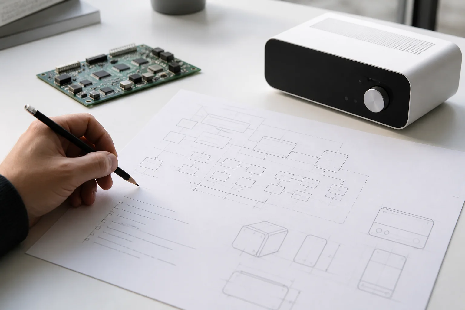
Every successful electronic product starts with a clear understanding of its requirements. In a PCB design service, the first step is translating product goals into a practical electronic design.
We work with customers to define the electrical, mechanical and functional requirements that shape the schematic, the PCB layout and the overall electronic design — before a single trace is routed.
-
Product Requirements
The electrical, mechanical, environmental, functional and cost requirements that drive the whole PCB design.
-
Component Selection
Selecting reliable, commercially available components matched to the electronic design — on performance, lifecycle and supply.
-
System Architecture
Defining how processors, power, sensors and communication interfaces relate — the architecture that underpins the schematic.
From Schematic to PCB
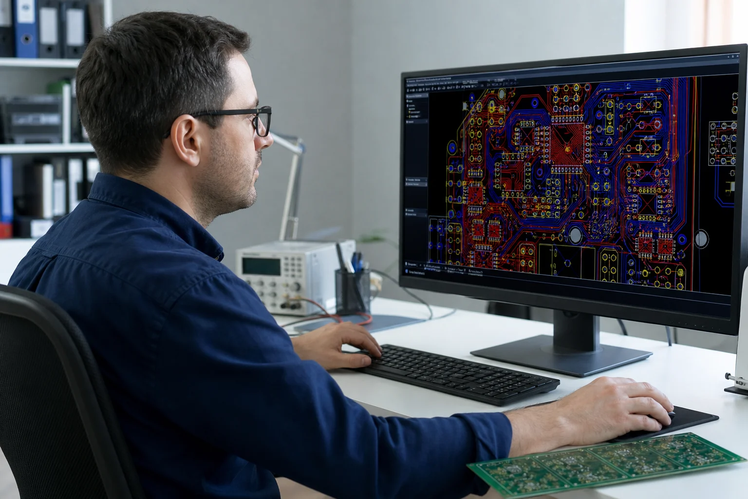
Once the architecture is set, our engineers move from schematic design to PCB layout — developing the electrical design and transforming it into a production-ready board.
Schematic Design
Developing complete electrical schematics — the foundation of the PCB design.
Component Selection
Selecting components for the electronic design on performance, availability, reliability and cost.
PCB Layout
Optimizing placement, routing, power distribution, grounding and signal integrity for a manufacturable PCB layout.
Design Review
Reviewing the PCB design for electrical performance, manufacturing feasibility and potential production risks.
Designed for Manufacturing and Testing
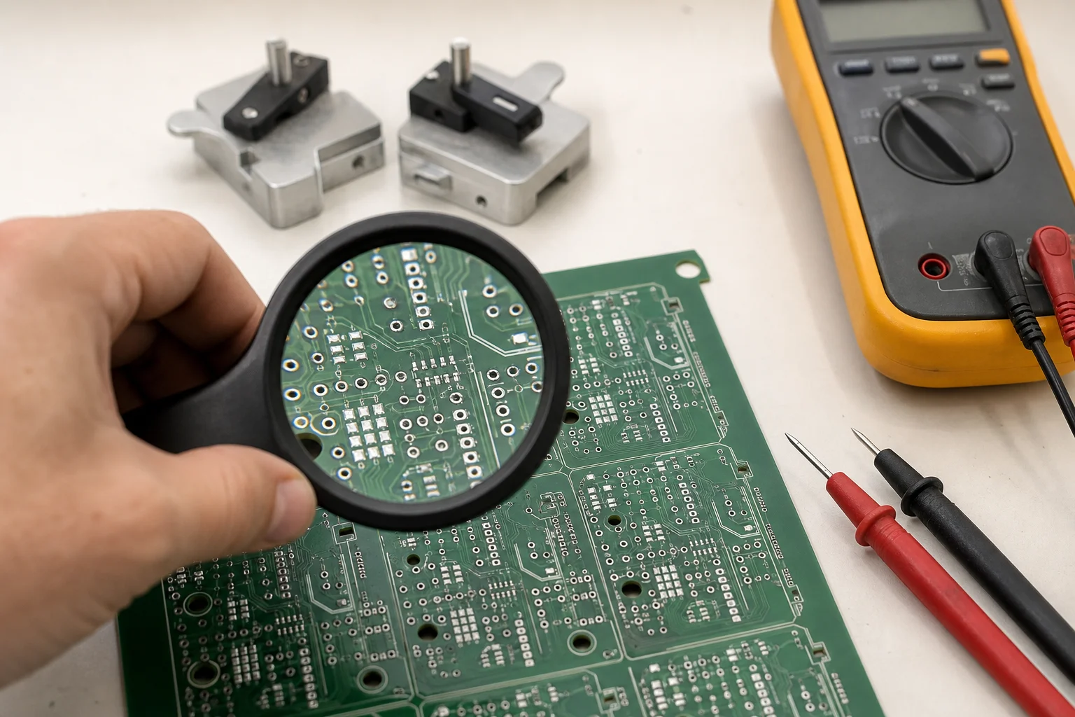
A PCB design that works in the laboratory may not be suitable for mass production — so DFM and DFT are built into our PCB design service from the start.
Our engineering team applies DFM and DFT to the PCB layout and schematic, catching manufacturing and testing issues before they reach production.
DFM
- Component spacing
- Pad design
- Soldering clearance
- PCB fabrication limitations
- Assembly feasibility
DFT
- Test point accessibility
- ICT requirements
- Functional test access
- Programming interfaces
Design Validation
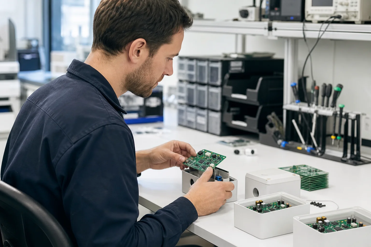
Before a PCB design moves into manufacturing, it is reviewed and validated — confirming the electronic design performs as intended and is ready for production, and reducing downstream risk.
Frequently Asked Questions
Answers to the questions we hear most about our PCB design service — what is included, how projects start and run, what you receive, why design with a company that also builds the boards, and the terms we use every day: DFM, DFT, design validation and more.
What does your PCB design service include?
Our PCB design service covers the full path from product requirements to a production-ready board: system architecture, schematic development, component selection, PCB layout with power distribution, grounding and signal-integrity optimization, design review, and DFM/DFT integration.
One team owns the design end to end, so performance, reliability and manufacturability are considered from the first drawing — not checked at the end.
Can you start a project from just a product idea, without design files?
Yes. Many projects begin with nothing more than a product concept. We work with you to define the electrical, mechanical, environmental and functional product requirements first, then translate those goals into system architecture and schematic before a single trace is routed.
If you already have a design, we can instead take over the existing schematic, netlist, BOM and PCB layout files and carry them forward.
How long does a PCB design project take?
Timelines depend on board complexity, layer count and your target date. A typical simple design moves from requirements review to production-ready files in a matter of weeks, while complex multi-layer or high-speed designs take longer.
We provide a milestone-based schedule after the initial product requirements review, so you can track progress at every stage.
What deliverables do we receive when the design is complete?
A complete design package, typically including: final schematic, PCB layout files, netlist, BOM, Gerber/fabrication files, design review and DFM/DFT reports, and documentation for prototype and mass production.
The exact deliverable list is confirmed in the project agreement.
Why design with a company that also manufactures the boards?
Because the design is built for the production line from day one. Our in-house PCB manufacturing, SMT & THT assembly, test, NPI and mass-production teams review your design during development, so manufacturing and testing constraints are caught while they are still cheap to fix — in the design stage — rather than on the production line.
When your design is released, it goes straight to our NPI flow without handoff delays.
What is DFM (Design for Manufacturing)?
DFM — Design for Manufacturing — is a structured review of the PCB design that checks whether it can be built reliably and cost-effectively at volume. A design that works in the laboratory may not be suitable for mass production, so DFM is applied before prototyping begins.
In our PCB design review we check component spacing, pad design, soldering clearance, PCB fabrication limits and assembly feasibility, so problems are fixed in the design stage where they are cheap — not on the production line where they are costly.
How does design validation work?
Design validation is the stage between finishing a PCB design and releasing it for manufacturing. Its purpose is to reduce downstream production risk before any boards are built.
A PCB design moves through five checkpoints: electrical verification of the circuit, a full PCB design review, prototype preparation, a manufacturing review against the fabrication and assembly process, and a final production-readiness confirmation. Only a design that passes all five checkpoints is released for production.
What files are required to start a PCB design project?
It depends on the stage of your project. From an early stage we can start a PCB design project with your product requirements — electrical, mechanical and functional specifications, operating environment and target cost. From an existing design we usually work from the schematic, netlist, BOM and PCB layout files.
In either case our engineering team reviews the complete design package before it moves to prototype or manufacturing, so the electronic design is confirmed ready for production.
What is DFT (Design for Test)?
DFT — Design for Test — makes sure a PCB can be tested reliably once it is assembled. A design that cannot be tested cannot be released for production, so testability is built into the PCB layout from the start.
Our DFT review covers test point accessibility, ICT (In-Circuit Test) requirements, functional test access and programming interfaces such as firmware and configuration access.
What is the difference between a prototype and a production-ready PCB design?
A prototype proves the PCB design works. A production-ready design has additionally been verified to be manufacturable and testable at volume, having passed DFM, DFT and design validation. That is what separates an engineering build from a stable, repeatable production design.
Have a Design in Mind?
Whether you have complete engineering files or an early-stage product concept, our team can help prepare it for reliable manufacturing.
Talk to Our Engineers